A comprehensive research whitepaper on critical interface technology in semiconductor, consumer electronics, aerospace, and advanced EV applications.
In the contemporary electronics landscape, where circuit density and signal speed continuously scale, electronic test probes represent the ultimate physical interface between complex electrical assemblies and automated test systems. As components shrink and the demand for absolute signal integrity peaks, engineering-driven sourcing departments are shifting away from generalist component brokers. Instead, they seek strategic wholesale partnerships capable of delivering highly specialized test probes that guarantee low contact resistance, extreme structural fatigue life, and compliance with high-frequency limits.
At the macro level, the global demand for electronics testing interfaces is undergoing structural expansion. The rise of multi-chip packaging, advanced high-power semiconductor architectures, automotive driver assistance systems (ADAS), and IoT connectivity protocols requires absolute structural reliability. The modern PCB assembly lines of tier-one electronics manufacturers are tasked with conducting rapid, accurate testing methods including In-Circuit Testing (ICT), Functional Testing (FCT), and high-frequency RF verification. Achieving this without introducing measurement anomalies or damaging delicate test points requires a deep understanding of metallurgy, spring dynamics, and interface geometry.
For procurement professionals and hardware engineers to choose the correct wholesale electronic test probes, it is critical to classify these elements based on operational criteria:
The performance profile of any test probe is determined by its material composition. Selecting the correct tip geometry, plating, and spring material defines whether a testing setup succeeds or fails on the production floor.
Serrated tips break through oxides on solder pads. Crown tips center themselves on component pins. Pointed configurations pierce through conformal coatings without sliding off target centerlines.
Using Beryllium Copper (BeCu) for structural tips ensures shape retention under high-duty cycles. Nickel-silver or gold-plated brass barrels prevent high thermal resistance and minimize friction.
Music wire or stainless steel springs, plated in premium gold, maintain reliable contact pressure. Consistent spring rate limits deflection under high repetition runs.
Under heavy production use, test probes suffer from electrical contact deterioration. As thousands of cycles build up, contamination builds on the tip surface, increasing contact resistance. Gold and rhodium coatings help maintain low milliohm resistance. Choosing the right plating material is crucial for automated testing fixtures, ensuring they do not generate false failures that disrupt production output.
Machine-Win Technology Co., Ltd. is a professional and reliable international supply chain partner specializing in sourcing high-performance solutions for global electronics manufacturers. With extensive experience and a globally interconnected network of suppliers, we excel in delivering premium quality testing systems, electronics, electricals, and mechanical spare parts.
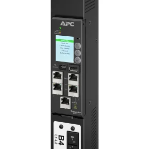
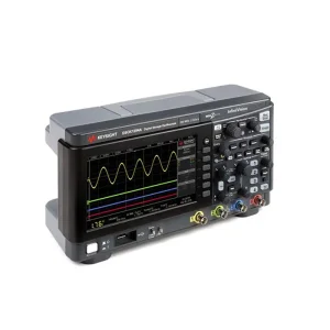
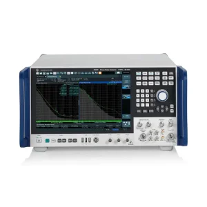
We serve as your strategic partner for instrument sales, repair, and calibration, as well as network testing solutions. Our product catalog covers leading names in the test and measurement landscape, including KEYSIGHT, R&S, TEKTRONIX, KEITHLEY, RIGOL, NI, MEGGER, DRUCK, YOKOGAWA, ITECH, and more. From advanced oscilloscope setups and network analyzers to high-speed contact probes, our network guarantees genuine components, precise technical specifications, and seamless execution.

Precision testing needs vary across different target industries. The application requirements below outline the unique demands on test probe design and reliability.
Electric vehicles run high-voltage drivetrains and critical ADAS control boards. Sourcing probes for this sector requires high thermal tolerance and the capacity to carry large current flows during functional testing, all while preventing arcing or damage to sensitive electronic components.
Testing RF and 5G transceiver setups requires impedance-matched coaxial probe configurations. Sourcing focuses on low-loss connectors, precise 50Ω path matching, and consistent mechanical alignment to prevent signal reflection at high frequencies.
Smartphones and wearables pack micro-scale electronics onto high-density PCBs. Testing these tight layouts requires fine-pitch contact probes with small tip diameters, configured to run smoothly in high-volume, automated assembly environments.
Sourcing electronic test probes in volume introduces unique supply chain challenges. Substandard copycat brands often compromise on plating thickness, leading to early contact degradation and high false-failure rates on assembly lines. OEMs and EMS providers can address these risks by partnering with suppliers who offer clear materials documentation, verified dimensional accuracy, and testing support.
Bringing equipment, original parts, and supply chain logistics together into a single, cohesive service platform.
We source across top equipment catalogs, including KEYSIGHT, Rohde & Schwarz, Tektronix, and Megger, saving procurement teams valuable time and administrative overhead.
We provide full calibration support to ensure your acquired testing instruments and probe interfaces meet international tolerance standards.
Our technical team coordinates custom probe designs, shielding configurations, and material changes to match unique project requirements.
Precision testing probes operate in demanding regulatory environments. Standard compliance is essential for products heading to sensitive industries like medical electronics, automotive, and defense equipment.
We supply probes compliant with RoHS and REACH regulations, avoiding heavy metal pollutants like cadmium and lead. This is critical for consumer and medical electronics manufacturing.
Our testing devices and probes align with ISO 9001 and ISO/IEC 17025 testing metrics, providing traceability that helps simplify your quality control audits.
Unplanned logistics delays can disrupt production line setups. Machine-Win mitigates this risk by managing custom clearances, providing secure packing to prevent tip deformation, and running active tracking for international freight. Our team maintains communication throughout the delivery process, ensuring test engineering projects stay on track.
The testing interface landscape is changing to keep pace with next-generation electronics. Sourcing teams can stay ahead by preparing for these key developments:
Advanced packaging designs like chiplets and high-bandwidth memory (HBM) are driving testing contacts down to ultra-fine pitches. Standard spring probes are being replaced by micro-cantilever and vertical probe architectures to handle tighter space constraints.
With Wide-Bandgap (WBG) semiconductors like Gallium Nitride (GaN) and Silicon Carbide (SiC) seeing wider use, probes must carry higher currents and withstand voltage spikes without melting. This requires new composite alloy tips and heat-resistant spring components.
Future testing setups will incorporate smart probes capable of tracking local temperatures and cycling counts, helping engineering teams predict wear and schedule maintenance before failures occur.
Technical guidance to help sourcing teams select the right testing interfaces.
Tip selection depends on the contact point: use pointed tips for penetrating flux or conformal coatings on vias, crown tips for component pins, flat tips to avoid leaving marks on soft surfaces, and cup/serrated tips to establish reliable contact with spherical solder joints.
Contact resistance rises due to oxidation, tip wear, and debris buildup. You can mitigate this by choosing hard, gold-plated tip alloys (like Beryllium Copper), using serrated tips that help clear away surface residue, and establishing a regular maintenance and cleaning routine.
Industrial-grade spring probes typically range from 500,000 to over 1,000,000 compression cycles. Actual lifetime depends on operating temperature, side loads, lateral stress, contamination, and contact force.
Yes. Our sourcing network supports custom probe specifications, including variations in spring force, body dimensions, plating thickness, and pitch spacing for high-density testing applications.
Standard probes feature a single current-carrying contact. Kelvin probes house two isolated electrical pathways within one probe body, enabling four-wire resistance measurements that filter out lead resistance to provide highly precise low-ohm readings.